This is not intended to be a comprehensive introduction. It ignores Band Theory and any distinction between valence and conduction bands. It is intended to give a simple (you may be justified in claiming it is over-simplified) concept of how extrinsic semiconductors, and devices that employ them, work.
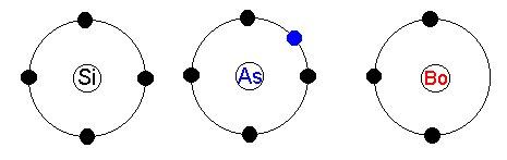
Pure silicon and germanium are "intrinsic semiconductors", that is they are "naturally" semicondiuctors. In order to make devices like diodes and transistors, the quality of their semiconductor nature needs to be controlled, and their conductivity needs to be slightly increased. This is achieved by "doping" the intrinsic semiconductor with tiny amounts of impurity atoms that are similar in size to the semiconductor atoms, but which have more (e.g. Arsenic) or fewer (e.g. Boron) valence electrons:
So, we begin with a crystal of pure silicon:

and add some pentavalent impurity (e.g Arsenic):
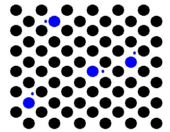
Only four of the valency electrons of the arsenic are needed to bond with the silicon in the crystal lattice. The others are effectively free and can take part in conduction. The doping impurity atoms are called donors because they enable the crystal to donate electrons. Electrons carry a negative charge, so this type of extrinsic semiconductor is called n-type.
An alternative is to dope the silicon with a trivalent impurity (e.g. Boron):
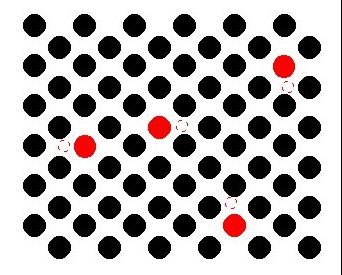
The boron has only three valence electrons, one fewer than is needed to complete the bonding in the crystal lattice, so there are effectively "holes" where the "missing" electrons are. The doping impurity atoms are called acceptors because they enable the crystal to accept electrons. These holes can be seen as carriers of positive charge, since they are "absence of electrons". This is a p-type semiconductor.
If there is a junction between p-type and n-type material in the same continuous crystal lattice:
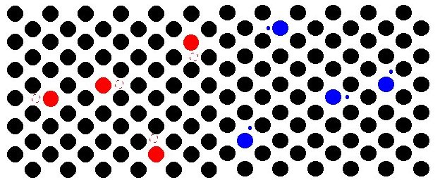
electrons near the junction migrate (by diffusion) into holes:

Because electrons have left the n-type material, it becomes positively charged. Similarly, the p-type material becomes negatively charged. These charges prevent the further diffusion of electrons into the p-type layer and of holes into the n-type layer. This region is therefore almost free of charge-carriers (holes or electrons) and is effectively an insulator.It is called the depletion layer or barrier layer. It is less than 10-6m wide and, because of the charges, behaves as if there was a voltage across it. This junction voltage is typically a few hundred millivolts.
If a battery is applied across a p-n junction with the positive terminal connected to the n-type side (this is called reverse bias)and the negative terminal applied to the p-type side, this helps the junction voltage, and the depletion layer is widened. Only a few minority carriers (holes from the n-type or electrons from the p-type, produced by bonds breaking at room temperature) cross the junction as a leakage current or reverse current.

If the battery is connected the other way round, in opposition of the junction voltage, the depletionlayer narrows. When the applied voltage exceeds the junction voltage, a large current flows because the electrons and holes are able to cross the junction:

We have a semiconductor diode.
Diodes are commonly used in rectifier and diode-logic circuits.